Doppler Product Design and Manufacturing

Occasionally we are asked about how we build and test our products. So, I thought I’d share a little about our design and manufacturing process.
We design all our products locally using in house engineers and some outside consultants. This includes all the schematic design, printed wiring board design and mechanical drawings of our antennas. Additionally we develop our own firmware and our software. During the design process we work with our vendors to insure manufacturabililty.
We typically build and test a few prototypes and test them during the design process. We make the necessary tweaks to the design until we are satisfied that it meets requirements.
We then produce a first article that we exhaustively test it to make sure it performs to specifications.
We use outside vendors to produce all of our piece parts and sub-assemblies and we do final assembly and test at our facility in Carefree, AZ. All our primary vendors are in the United States and most are in the local Phoenix area. This includes our machine shops, plating vendor, circuit board vendor, electronic circuit assembly vendor, cable vendor and our powder coat vendor. We have a long relationship with all these vendors and they have performed admirably throughout the years.
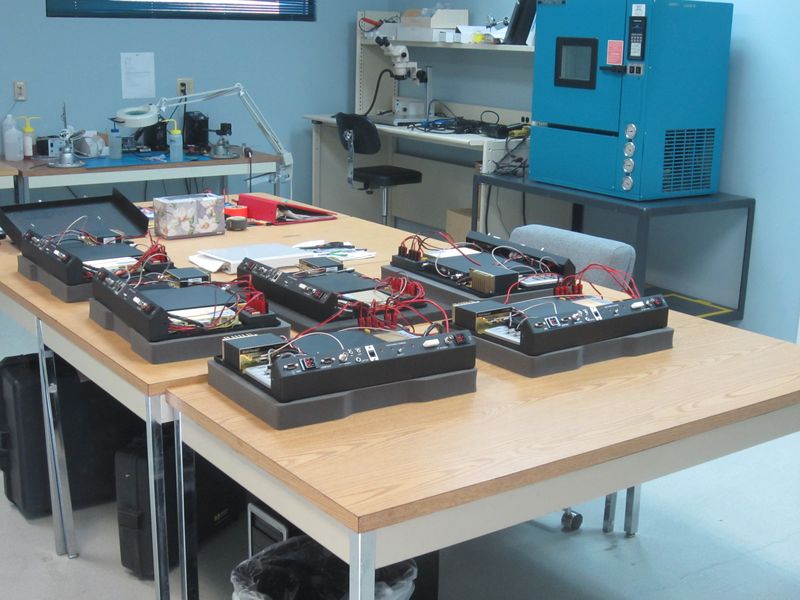
Final assembly and test takes place in our facility and consists of
- Programming the antenna FPGA
- Calibrating each antenna board so the antennas are precisely gain matched
- Assembling the antenna circuit boards into the antenna housings
- Mounting connectors on the antenna housings
- Assembling the processor circuit card assemblies into their housings
- Programming the DF processor FPGA and firmware
- Then each final assembly is 100% tested using written test procedures
Our results speak for themselves. In the last five years, we’ve only had one unit returned for repair.